** MAIN FEATURES **
** BEAMS **
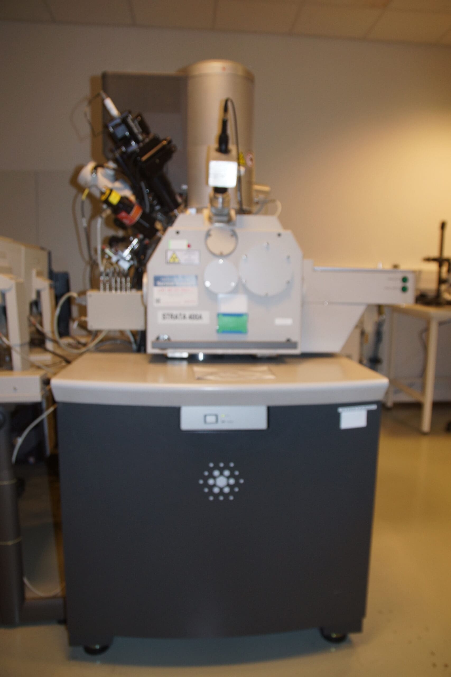
Electron source Schottky thermal field emitter
Ion source Gallium liquid metal
Beam voltage
SEM 200 V – 30 kV
FIB 500V – 30 kV
** RESOLUTION **
Visual resolution@ 1kV : 2.5nm
Visual resolution@ 15kV : 1 nm
** DETECTORS **
ETD (chamber)
CDEM (chamber)
TLD (In-lens)
** STAGE **
X and Y repeatability at 0° tilt inf 0.5 µm
** GIS **
Insulator Enhanced Etch
Tungsten
insulator dep
** ACCESSORIES **
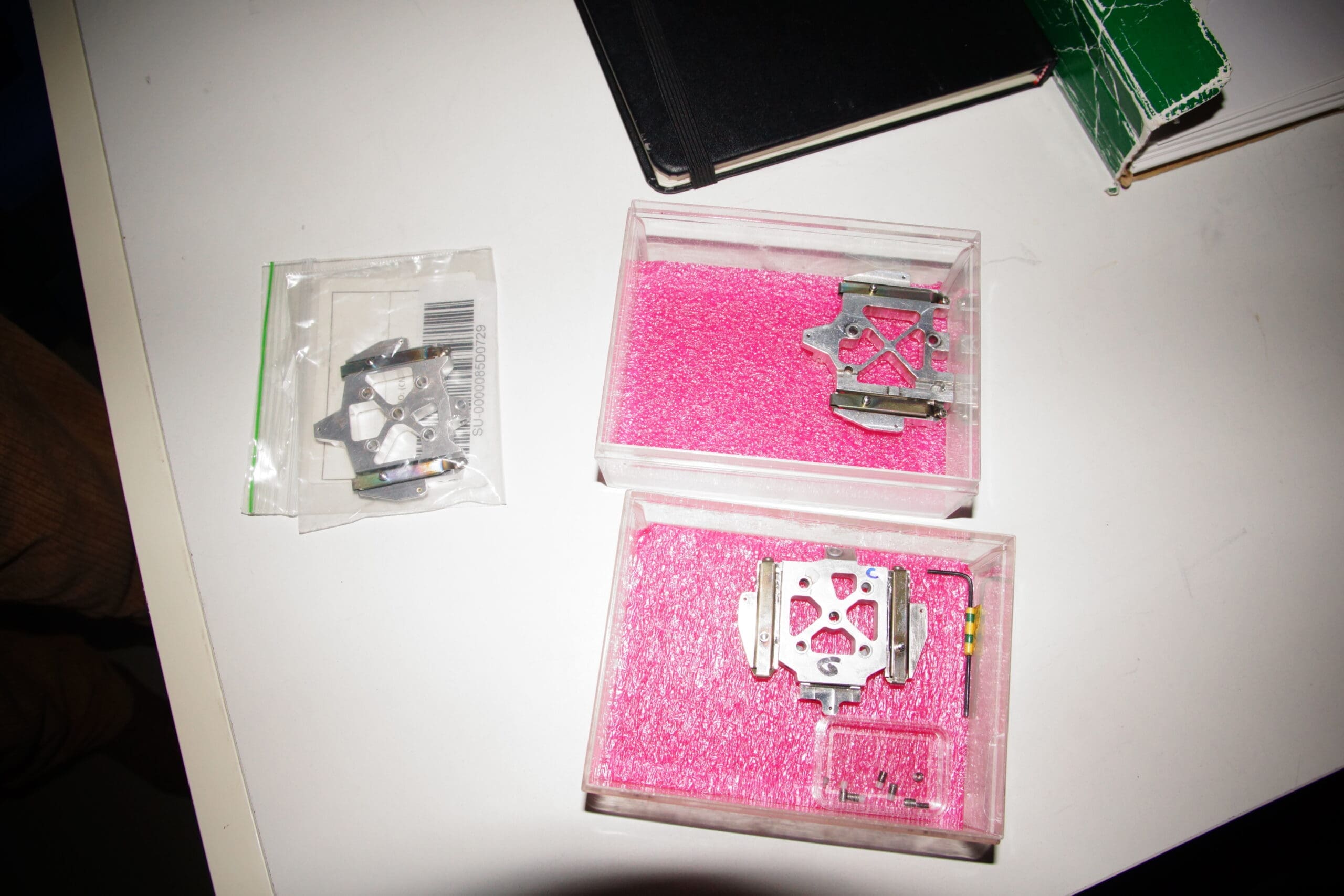
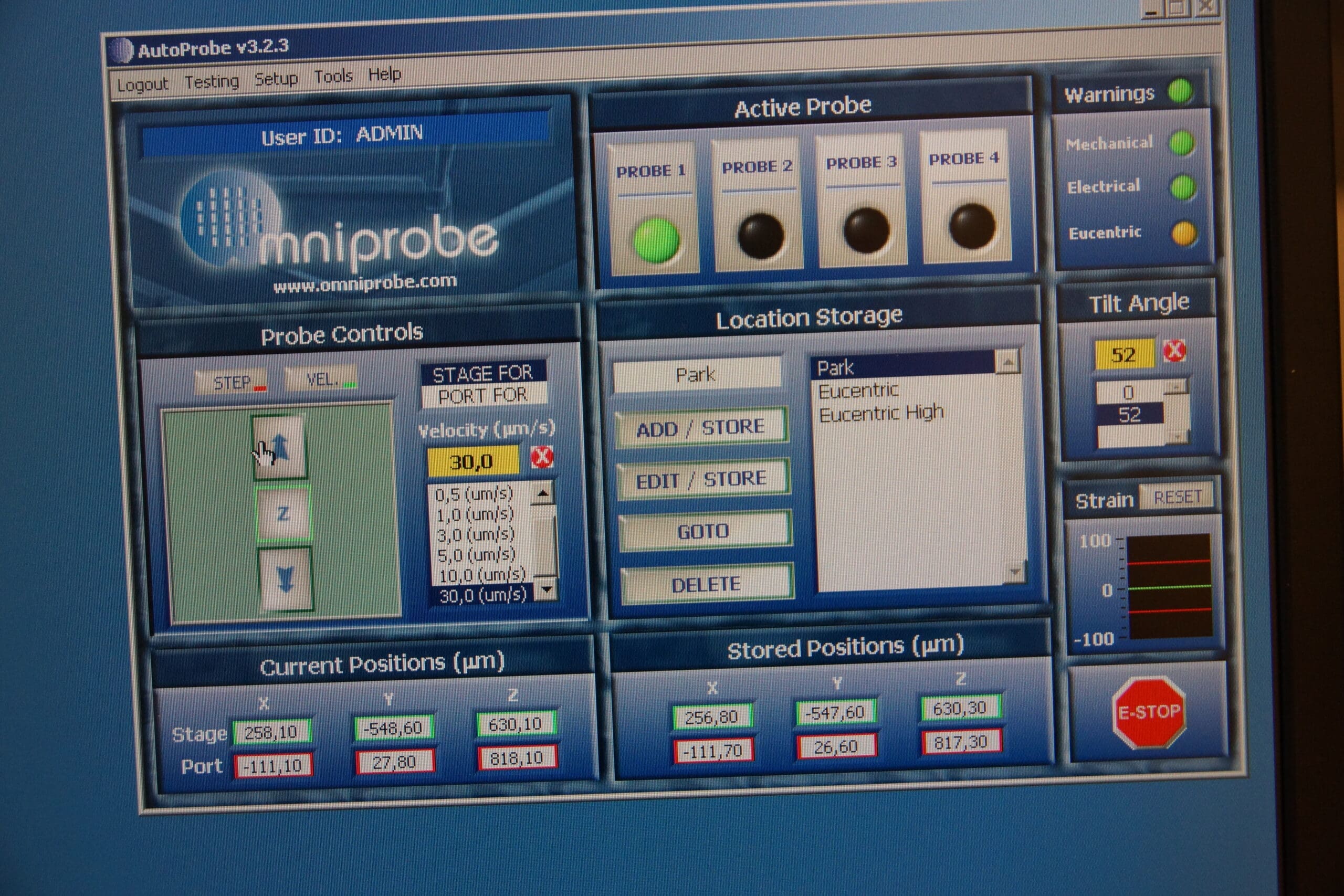
Micro manipulator: Omniprobe 200
support PC
water chiller
Oneac transformer
Sample types Wafer pieces, packaged parts
Max sample size 75 mm diameter, loadlock compatible
In-situ section extraction system
User interface Windows 2000® GUI with integrated SEM, FIB, GIS,
imaging and patterning
Simultaneous patterning and imaging mode


