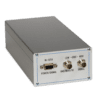
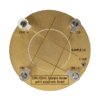
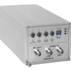
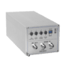
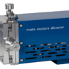
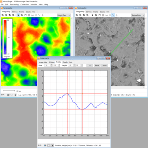
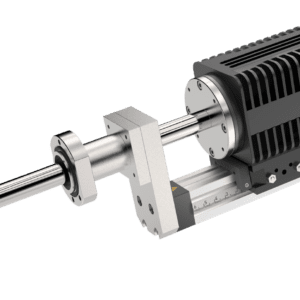
EA amplifiers are complex multi-stage amplification systems with integrated current & voltage sources for Electrical Analysis. All versions feature a high-speed transimpedance preamplifier for imaging, a bandwidth filter and a flexible second-stage amplifier for imaging. High-precision voltage and current sources are integrated into the compact housing, as required for biasing, IV sweeps and compensation. Packaging is miniaturised in order to reduce cable lengths, increase speed and optimise signal-to-noise ratio.
Standard features
* High-speed and low-noise ex-situ preamplifier with adjustable gain
* Automatic routing, to ground, bias or beam current meter
* Lowpass filter to match amplification with imaging speed
* Second-stage amplifier for fine image adjustments
* Voltage source for device biasing
* Current source to compensate for forward or reverse signals
* Auto-zero function for calibration
Optional features
* In-situ preamplifier for low impedance samples (with the Premium EA sample holder)
* Automatic current – voltage sweeps for device characterisation
The amplifer is part of the EA for SEM system and is designed for a wide range of Electrical Analysis techniques.
Versions
1. EA amplifier
* ex-situ preamplifier for junctions and Schottky barriers
* fully calibrated electronics for quantitative technique
2. Lock-in EA amplifier
* integrated clock generator for beam blanker
* ex-situ preamplifier for junctions and Schottky barriers
* analog lock-in amplification with de-modulation
Control
* USB2 hardware interface
* device driver for Microsoft Windows
* independent control library
* integrated DISS control panel
Inputs
* HIGH input for sample signal
* LOW input for sample gound
* DC input power (back panel)
* GND input (case)
Outputs
* Amplified output for imaging (back panel)
* LOW output for bias voltage
* BC output for external beam current measurement
* EBAC output for in-situ electronics
Ex-situ preamplifier
* 20,000 Ohm minimum sample resistance
* 10^3 … 10^10 V/A configurable gain
* 8 µs minimum pixed dwell time, depending on sample impedance
* 12-bit ADC for live signal inspection
In-situ preamplifier (optional)
* 1,000 Ohm minimum recommended sample resistance
* 10ˆ7 V/A fixed transimpedanced gain
* 16 µs minimum pixed dwell time, depending on sample impedance
Second-stage amplifier
* -1 … 1 µA, 16-bit input offset (brightness)
* 0.1 … 100x, 16-bit gain (contrast)
* 0.5 MHz at 10^9 V/A bandwidth
* 8-levels low-pass filter
* manual signal inversion
Integrated sources
* -10 … 10 V, 16-bit voltage bias
* -10 … 10 µA, 16-bit current compensation
* 100 pA internal source for calibration


